
Thermal Clad
Introduction / Benefits
Thermal Management Substrate, Im

Electronics of the future brings demanding new challenges that need innovative new answers.
Thermal Clad is one of these answers. It is a material that considers heat transfer as a design requirement.
As devices get smaller and power goes higher, electronics designers need to continually challenge traditional methods of design to develop more reliable product designs. Thermal Clad’s applications run from semiconductor modules to power supplies and motor controls.

WHY USE THERMAL CLAD?
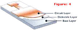
THERMAL MANAGEMENT SUBSTRATE, IM
Thermal Clad is used as a substrate, heatsink and /or printed circuit material.
In the design phase, the engineer considering the use of Thermal Clad should evaluate the new design in light of the potential to:
- Improve product thermal & physical performance
- Combine power and control
- Increase power density
- Improve product durability
- Enable better use of surface mount technology
- Reduce heat sinks and other mounting hardware, inluding thermal interface material
- Reduce printed circuit board real estate/interconnects
- Replace fragile ceramic substrates with greater mechanical durability
- Cost effectively obtain " odd shaped " parts
- RoHS compliant
- Lower operating temperature
- Extend life of dies
LED Thermal Management
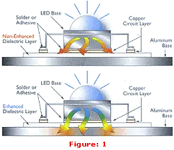
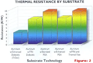
In a typical LED configuration (Figure 1), heat generated by the LRD lamp is transferred to the base metal through the dielectric layer. However, most dielectrics selected for this purpose have little or no thermal conductivity to move heat away from the assembly and into the heat spreader (the metal base). Often referred to as enhanced dielectric, T-Clad™ minimises thermal impedance and conducts heat more effectively and efficiently than standard printed circuit boards (see Figure 2).
| Material | Description | Advantages |
|---|---|---|
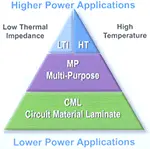
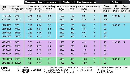
| HT | 2.2 W/mK. Better thermal performance. High Tg epoxy formulation. Purchased as panels, parts or coated onto foil. Available in 0.003" to 0.006" thickness dielectric. | • Same thrmal performance as LTI with the added benefit of very stable electrical properties at high temperature. |
| LTI | 2.2 W/mK. Better thermal performance. Standard epoxy formulation. Purchased as panels, parts or coated onto foil. Available in 0.003" to 0.006" thickness dielectric. | • Offers lower thermal impedance (~25%) in the application • Used formally in conjunction with copper base formaximum thermal performance. |
| MP | 1.3 W/mK. General purpose dielectric. Standard epoxy formulation. Purchased as panels, parts or stand-alone laminating material. Available in 0.003" to 0.006" thickness dielectric. | • Flexible and robust. • Fits most application well. • Uses - Power, motor controls, etc. |
| CML | 1.1 W/mK. Epoxy coated fiberglass. Standard epoxy formulation. Purchased as panels, parts or stand-alone laminating material. Available in 0.006" thickness dielectric. Can be stacked two high for 0.010" to 0.012" dielectric. | • Easy to handle for custom-built parts. • Supplied as prepreg in sheet or roll form. |
SUPPORT FAQs
Common Questions About Our Products
How does the cost of Thermal Clad compare to those of FR4?
How does the cost of Thermal Clad compare to those of DBC?
Our company does not do surface mounting. Can we still use Thermal Clad?
Do I need an interface between Thermal Clad and any additional heat sink?
Why do you offer copper based as well as aluminium based Thermal Clad?
What circuit finishes are available?
Do I need to fix my power devices in place during re-flow to stop them moving around?
I would like to have some parts to test. How do I go about getting prototypes?
You simply contact us. Bergquist can take care of all of your prototype needs. Obviously we can supply them ourselves, but we also have a network of local printed circuit shops familiar with processing Thermal Clad. They can supply prototypes on our behalf or you can work directly with them.
All you need to get started is:
- Circuit pattern layout (preferably in electronic format i.e. Gerber)
- Mechanical design giving:
- positions for fixing holes and their size
- overall dimensions and
- importantly a dimension linking the artwork traces to a mechanical feature.
(i.e. dimensions of fidusial to datum edges) - The material specification
- The required finish will complete the information we need